The NIMFEIA consortium unites three universities, three research centers, and two industry partners.
Together they possess complementary expertise covering a wide range from basic research in magnetism and spintronics to product development in the microelectronics sector.
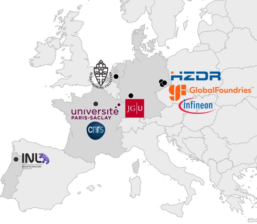
The NIMFEIA project is coordinated by the Helmholtz-Zentrum Dresden-Rossendorf e.V. (HZDR) in Germany.
HZDR performs – as an independent German research center – research in the fields of energy, health, and matter. The focus lies on answering the following questions:
- How can energy and resources be utilized in an efficient, safe, and sustainable way?
- How can malignant tumors be more precisely visualized, characterized, and more effectively treated?
- How do matter and materials behave under the influence of strong fields and in smallest dimensions?
To help answer these research questions, HZDR operates large-scale facilities, which are also used by visiting researchers: the Ion Beam Center, the Dresden High Magnetic Field Laboratory, and the ELBE Center for High-Power Radiation Sources. HZDR is a member of the Helmholtz Association and has six sites (Dresden, Freiberg, Görlitz, Grenoble, Leipzig, Schenefeld near Hamburg) with about 1,500 members of staff, of whom about 670 are scientists, including 220 Ph.D. candidates.
HZDR is represented by Dr. Katrin Schultheiss, an expert in the area of magnonics with special emphasis on nonlinear magnon-magnon interactions. She is a member of the Department of Magnetism, which specializes in the study and characterization of magnetization dynamics and provides facilities for extended ferromagnetic resonance (FMR) studies, magnetic characterization (SQUID, VSM), magneto-optical characterization (Brillouin light scattering, time-resolved magneto-optical Kerr effect), cleanroom standard UV- and e-beam lithography and dedicated ion-milling facilities for nano-fabrication, high-frequency spin-transfer-torque characterization up to 50 GHz including real-time magnetic switching, spin-torque, and thermally-excited FMR analysis.
Research on micromagnetic modeling is conducted at the Centre for Nanoscience and Nanotechnology – a joint research unit of the Université Paris-Saclay (UPS, Beneficiary) and Centre National de la Recherche Scientifique (CNRS, Affiliated Entity), located in Palaiseau in the greater Paris area. The research activities of the institute are carried out along four main lines – nanoelectronics, photonics, materials science, and micro- and nanosystems – which are supported by one of the largest nanofabrication clean room facilities in France.
The group at Université Paris Saclay is represented by CNRS research director Dr. Joo-Von Kim, who has over 20 years of research experience in theoretical and computational magnetism. He is a member of the Novel Magnetics Devices Group, which possesses a strong track record in theoretical, computational, and experimental studies on magnetization dynamics in the GHz regime, such as spin-torque nano-oscillators, switching in magnetic memory elements, magnonics, and the dynamics of topological magnetic solitons (domain walls, vortices, skyrmions), where the scope of the research undertaken spans fundamental aspects to applications in information storage. In recent years, the group has expanded its expertise in computational magnetism with the development of a high-performance cluster and tools for solving multiphysics problems, which covers the chain from atomistic spin dynamics to large-scale micromagnetic simulations that also incorporate other features such as detailed electromagnetic and strain models of realistic device geometries. The group also collaborates with researchers within the institute in neuromorphic computing, whose expertise will feed into the project.
The Kläui Laboratory at Johannes Gutenberg-University Mainz (JGU) in Germany, headed by Prof. Mathias Kläui, is a key contributor to the development of advanced materials from in-plane magnetized disc systems hosting low pinning skyrmions with well-defined and reproducible magnon spectra to out-of-plane magnetized systems hosting complex skyrmions and finally to (synthetic) antiferromagnets.
With extensive experience in confined spin structures including the statics and dynamics of vortices and skyrmions as well as domains and domain walls in antiferromagnets, the real space time-resolved imaging capabilities provide full information on the spin structure dynamics as well as magnon properties. Beyond the materials structured into elements and the resulting spin structures and their dynamics, the group has been working on electrical detection of magnetic properties including the dynamics of vortices by homodyne detection and using tunneling magnetoresistance junctions for high amplitude sensing of spin switching and dynamics.
The team at Radboud Universiteit (RU) in the Netherlands, represented by Dr. Johan Mentink, is a key contributor to the theoretical and computational study of non-linear dynamics of magnetism in response to ultrafast laser excitation. The group closely collaborates with world-leading experimentalists aimed at understanding the mechanisms of ultrafast switching of magnetism. To this end, a stable and fast numerical time integration method was developed that is currently the default scheme in the widely used open-source software packages UppASD132 and SPIRIT133.
For the last 3 years, the group investigated the application of machine learning methods, to simulate the ultrafast dynamics of antiferromagnets following perturbations of exchange interactions. This directly accesses magnons at the edge of the Brillouin Zone, which opens up possibilities for faster and more energy-efficient control of nonlinear magnons beyond 100 GHz, with particular relevance for disclosing the scaling of the magnon reservoir computing concept in NIMFEIA and enhancing the reservoir capacity.
Infineon Technologies Dresden GmbH & Co. KG (IFD) in Germany, represented by Dr. Klaus Knobloch, will refine the application space of the technological approach of NIMFEIA.
GlobalFoundries Dresden Module One LLC & Co. KG (GF) in Germany, represented by Dr. Alexandra Titova, will be the main contact to align on the design requirements and judge the feasibility of NIMFEIA’s approach as a new AI accelerator. To test a first implementation, GF will provide space on multi-purpose wafers based on 300mm 22FDXTM technology.
The International Iberian Nanotechnology Laboratory (INL), represented by Dr. Alex Jenkins, is a new international research organization installed in Northern Portugal, and devoted to the development of nanotechnologies in the medical, environmental, and electronics areas. INL has a 1000 m2 state-of-the-art cleanroom facility for 200mm wafers which is regularly used for both research and industrial nanofabrication processes. Unlike the nanofabrication facilities which are common at many industrial and foundry facilities, INL’s role as a Research and Technology Organisation means they manage to balance throughput and performance as well as maintain the flexibility necessary to achieve challenging device processes such as those in NIMFEIA. INL is now running MEMS, spintronics, and hybrid devices on full 200mm wafers, and working on the integration of these devices with front-end CMOS wafers.
The Spintronics Research Group at INL is focused on the production of devices exploring the large magnetoresistance effect of CoFeB/MgO/CoFeB magnetic tunnel junctions (MTJs). The group’s research activity is developed around three pillars:
- High-frequency dynamics in MTJs: Exploring the magnetization dynamics in confined magnetic nanostructures, for both uniform and non-trivial magnetic textures, i.e. magnetic vortices, for a range of potential applications, including wireless communications, energy harvesting, and neuromorphic computation.
- Integration of MTJs with standard CMOS: The development of a nanofabrication process for sub-micron MTJs and the back-end process for the integration of MTJ pillars on standard CMOS circuits, including the high-frequency electrical characterization and electrical model creation of the devices produced.
- Magnetic field sensors and devices: Focusing on the optimization of MTJ stacks and linearization methods for CoFeB/MgO/CoFeB MTJs optimized for HDD read head sensors, sub-micron resolution field sensors, and general purpose low noise magnetic field sensors.